
I worked on this like a year ago, and probably the last DIY electronics project I did during recent times. I’m a music maniac and like anyone who loves enjoying music, I wanted a good music system (though I have one now). I had a couple of surround speakers lying around and thought I’d make good use of it if I could design a simple power amplifier. I was no good dealing with power transistors at that time, like MOSFETs so I decided on a chip amplifier. I couldn’t source components required for advanced builds so I stuck to a primitive(yet discontinued) chip from Sanyo. The LA4440 requires very little external components, a couple of electrolytic capacitors like any audio system.
And the funny part, I didn’t have a proper schematic. The datasheets were not reliable and didn’t elaborate much on its application. It only had graphs on its current draw with respect to gain, harmonic noise, operating temperatures and performance, etc. So I went back to where I found this chip first, a discarded amplifier board for use with a FM receiver. Thankfully, it was wired for a bridge config like the one I needed so I blindly, without interpreting how it all came together(well, I later did to fully understand how it worked) followed the traces on the PCB between each component and drew a rough schematic. This was proving to be tedious and there was this really dark-greenish solder resist making it even harder. I used ExpressPCB to draw my schematics for its simplicity. I wasn’t quite good at Eagle back then. The component libraries in ExpressPCB was something I was used to, making it easier to judge lead spacing and made designing custom components easier (cause this was a hybrid IC). The schematic below was the first one I drew (alpha stage? :-)). The big mistake here, the bridge rectifier used here was underrated. With a little help from the datasheet, I later realized at least 5 A was required to run the 6 stand alone channels in this amplifier. A 12 V DC power supply was required, so I included a plain old step-down transformer(12-0) with a rectifier (I was lazy to used diodes, and they could handle only 1 A current) along with a smoothing capacitor-cum buffer for leveling any ripple current and a ceramic cap for removing any noise. This power supply was way to simple and provided unregulated supply from a transformer. I later removed the power supply from this schematic and used the home power backup’s 12 V battery before switching to a laptop charger (I was desperate to find any source within my requirements).
Also during this time, I did extensive research and learning about band pass filters, high and low pass filters along with decoding and encoding 5.1 audio and pre amplifiers. And guess what, like always I came up with an idea of retaining every detail in music by using individual channels(microphone inputs) to record onto multiple standalone channels. The resulting file would be extremely large due to each channel having its own bit rate. These standalone channels are then encoded or compressed. While playing, after decoding, the separation of the channels are maintained without intermixing of sound signals. The channels are then played on specialized speakers or atleast the detail is retained.
I actually wanted to include a low pass filter to drive the sub, high pass to drive the tweeters and band pass for the center speaker which usually plays human voice in a 5.1 config. Although I was successful at initial schematics and finding the components I needed, I didn’t make it. One reason was the complexity of wiring and I couldn’t find the op amps required, though there were alternates, they were not audio specialized ’cause the ones I saw were low-noise and low-distortion ones (imagine distorting bass in your music… how annoying?!).
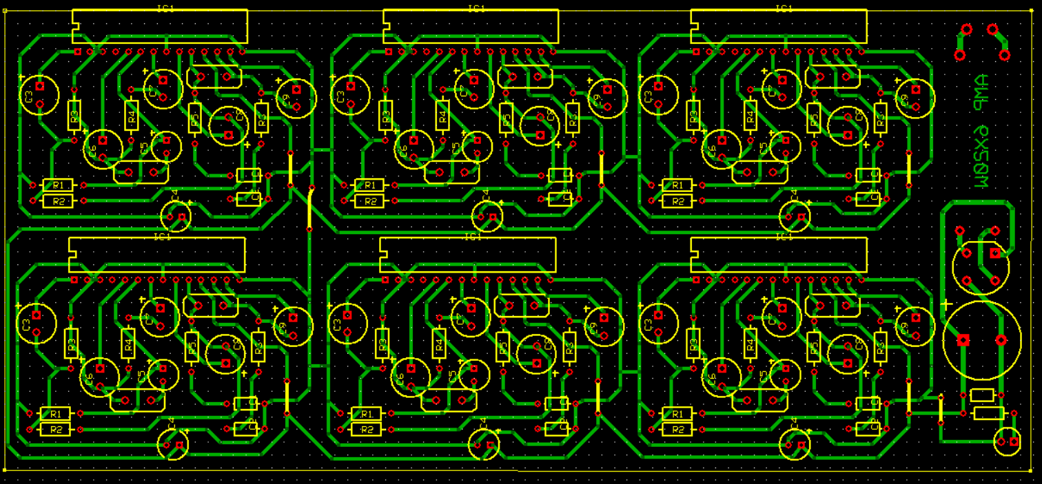
I fabricated the board using the mainstream DIY technique. I printed the artwork on A4 no-gloss photo paper. Why did I use A4 size? I didn’t want to loose scaling. My project files were scaled to A4. The copper clad board was single sided cause I didn’t have to deal with SMDs. After treating my board to some rubbing alcohol and kitchen fine scrubs, I used the toner transfer method to get my artwork transferred to the bottom of the board. I’m graceful not destroying the iron during the process. The board was removed of any paper residue and dropped in some freshly prepared Ferric chloride solution. After some serious agitation with the board submerged, while periodically checking if my board was turning transparent after all that excess copper is removed; I took it out, washed it under running water before using acetone and some kitchen tissue to scale off the plastic (toner) on the traces. I read online that drilling after tin coating the board would help you center the drill bit with ease, and yes it worked! The tin seemed to form a raised kind of surface around the solder pads making it easier to drill with a hand driller. A 0.8 mm bit was used for every hole on the board. Hand drilling the holes for the IC’s proved to be a challenging task. The fixed lead spacing between them means you’ve to get your drilling zeroed-in and inaccuracies would accumulate with others and cause trouble while soldering. Soldering was done with regular solder (60:40, tin:lead) and a hand-held soldering iron. Yea! that’s pretty obvious, who would wave solder a board this size. The aluminium heatsinks later went on with the chips stuck to them with thermal heat-conductive epoxy. The mounting holes were made using metal drill bit and lots of lubricant. Determining the hole locations required precision, I mean lots or your chip wouldn’t mount. A good method would involve using the datasheets to precisely know the dimensions and make holes accordingly, but I simply marked them with a pencil using the actual chip as a reference. The height was also a concern cause they had to perfectly go onto the PCB. Besides, I was super scared because I could mess up the whole thing… The heatsinks were sourced with much difficulty for its rare dimensions. I couldn’t find WD-40 so I instead used some coconut oil LOL. To reduce tension on the chip, I used only finger tight on the mounting bolts although the datasheet provides design maximums. To my surprise (and my expectation behind all this hard work), it worked!
I immediately played Leave Out All The Rest by Linkin Park, my fave song back then. I sourced the audio input from my phone, I ripped off the wire from the 3.5 mm headphone jack to reveal 3 wires (left channel, right, and ground) which I used to run this amp. It functioned till recently, one of the chips blew off due to a bridge between the traces. The PCB traces were left exposed since I didn’t have access to solder masking stuff. The pic below is the fully assembled board, guess I overused the thermal epoxy.

 Another interesting but pretty boring project which I did. I intended to use this for ambient lightning in my room and control the colored lights(in few numbers over the whites) with a PIC microcontroller but later dropped it when I found a good use for it. A night lamp first and now a light for my desktop keyboard, something mandatory for a nocturnal creature which blogs LOL.
